Solid State Electronics
Solid-state electronics means semiconductor electronics: electronic equipment using semiconductor devices such as transistors, diodes and integrated circuits (ICs). The term is also used for devices in which semiconductor electronics which have no moving parts replace devices with moving parts, such as the solid-state relay in which transistor switches are used in place of a moving-arm electromechanical relay, or the solid-state drive (SSD) a type of semiconductor memory used in computers to replace hard disk drives, which store data on a rotating disk.
The term "solid state" became popular in the beginning of the semiconductor era in the 1960s to distinguish this new technology based on the transistor, in which the electronic action of devices occurred in a solid state, from previous electronic equipment that used vacuum tubes, in which the electronic action occurred in a gaseous state. A semiconductor device works by controlling an electric current consisting of electrons or holes moving within a solid crystalline piece of semiconducting material such as silicon, while the thermionic vacuum tubes it replaced worked by controlling current conducted by a gas of particles, electrons or ions, moving in a vacuum within a sealed tube.
Although the first solid state electronic device was the cat's whisker detector, a crude semiconductor diode invented around 1904, solid state electronics really started with the invention of the transistor in 1947. The transistor was invented by John Bardeen and Walter Houser Brattain while working under William Shockley at Bell Laboratories in 1947. Before that, all electronic equipment used vacuum tubes, because vacuum tubes were the only electronic components that could amplify—an essential capability in all electronics.
The replacement of bulky, fragile, energy-hungry vacuum tubes by transistors in the 1960s and 1970s created a revolution not just in technology but in people's habits, making possible the first truly portable consumer electronics such as the transistor radio, cassette tape player, walkie-talkie and quartz watch, as well as the first practical computers and mobile phones. Other examples of solid state electronic devices are the microprocessor chip, LED lamp, solar cell, charge coupled device (CCD) image sensor used in cameras, and semiconductor laser.
Characteristics of PN Junction and Zener Diode
The PN junction diode is used for rectification purpose because it allows the current to flow only in one direction. It is a type of switch which only allows the forward current to pass through it. On the other hand, the Zener diode allows both the forward and reverse current to pass through it. The Zener diode is used as a voltage regulator in the electronic circuit because it provides the constant voltage from the supply to the load whose voltage vary over sufficient range.
Definition of PN Junction Diode
The PN junction diode is made up of semiconductor material. It is always conducted in one direction and hence used for rectification. The PN junction diode has two terminals namely anode and cathode. The current flows from anode to cathode.
The PN junction diode conducts only when it is connected in forward biased. The symbolic representation of PN junction diode is shown in the figure above. The arrow head represents the positive potential, and the bar shows the negative potential of the diode.
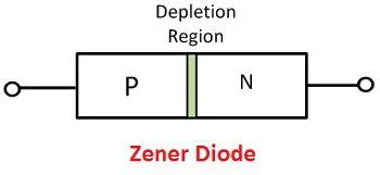
The PN junction diode has a P-type and N-type semiconductor material which is joined by the process of alloying. Thus, both the ends of the diode has different properties. The electrons are the majority charge carrier of the N-type material, and the holes are the majority charge carrier of the p-type semiconductor material. The region in which both the p-type and n-type material meets is known as the depletion region. This region does not have any free electrons because electrons and holes combine with each other in this region.
The depletion region is very thin, and it does not allow the current to flow through it. The PN junction starts conducting when the forward bias is applied across the junction. The forward bias means the P-type material is connected to the positive terminal of the battery and the N-type material is connected to the negative supply.
The forward biased creates the electric field which reduces the depletion region of the PN-junction diode. When the potential barrier is completely reduced, it creates the conducting path for the flow of current. Thus, large current starts flowing, and this current is called the forward current.
Definition of Zener Diode
The Zener diode is made up of silicon material. It is a special type of diode which operates in the breakdown region. It allows the current to flows both in the forward as well as in the reversed direction, when the Zener voltage is reached. The Zener diode is made by highly doped p-type and the n-type material, i.e. the concentration of ion is higher in the material.
When the reversed voltage is applied to the material, the depletion layer become reduces. Because of the thin depletion region, the concentration of the electric field is high. If the value of reverse voltage increases then the ions come out from the electrons and make the depletion region conductive. This breakdown of the depletion region is called the Zener breakdown and the voltage at which the breakdown occurs in known as the Zener voltage.
Key Differences Between PN-Junction and Zener Diode
The following are the key differences between the PN junction and Zener diode.
1. The semiconductor which conducts only in one direction is known as the PN-junction diode. And the Zener diode is the silicon diode which is optimised to operate in the breakdown region.
2. The reverse current flow through the diode damage the PN-junction diodes. The reverse current flows through the diode when it is connected in reverse biased. The reverse biasing means the p-type material is connected to the negative terminal of the supply and the n-type material is connected to the positive terminal of the supply. But the Zener diode allows the current to pass through both the direction.
3. The doping level of the PN-junction diode is low as compared to Zener diode. The width of the depletion region depends on their doping level. If the doping level of the diode is high, their depletion region is low and vice versa.
4. The breakdown in PN-junction diode occurs at high voltage level, whereas in PN-junction diode it occurs at low voltage levels. The breakdown is the phenomenon of making the depletion region conductive. The heavily doped diode has a low depletion region.
5. The PN-junction obey the ohm’s law whereas Zener diode does not obey the ohms law. The ohms law said that the voltage applies across the diode is equal to the product of the current and resistance applied across the diodes.
6. The PN-junction diode is mainly used for rectification purpose, whereas the Zener diode is used for providing the constant voltage to the load whose voltage vary.
Tunnel Diode
A tunnel diode or Esaki diode is a type of semiconductor diode that has effectively "negative resistance" due to the quantum mechanical effect called tunneling. It was invented in August 1957 by Leo Esaki, Yuriko Kurose, and Takashi Suzuki when they were working at Tokyo Tsushin Kogyo, now known as Sony. In 1973, Esaki received the Nobel Prize in Physics, jointly with Brian Josephson, for discovering the electron tunneling effect used in these diodes. Robert Noyce independently devised the idea of a tunnel diode while working for William Shockley, but was discouraged from pursuing it. Tunnel diodes were first manufactured by Sony in 1957, followed by General Electric and other companies from about 1960, and are still made in low volume today.
Tunnel diodes have a heavily doped positive-to-negative (P-N) junction that is about 10 nm (100 Å) wide. The heavy doping results in a broken band gap, where conduction band electron states on the N-side are more or less aligned with valence band hole states on the P-side. They are usually made from germanium, but can also be made from gallium arsenide and silicon materials.
What are transistors?
A transistor can be defined as a three-terminal device made up of semiconductor material that can act either as a conductor or insulator(based on the connection made) when the external potential is provided to its terminals. Basically, two different types of charge carriers are responsible for conduction in transistors, thus it is also known as a bipolar diode. This signifies the transfer of resistance from one part of the circuit to another. Due to its ability to change its state, it possesses two fundamental functions that are switching and amplification. Thus transistors can also be defined as electronic devices that can be used as switches when you could use a small amount of current to drive a larger current, to power something let's say like a light-emitting diode or you could use them to amplify a small AC signal.

We are going to talk about two types of transistors: the NPN transistor and the PNP transistor. These transistors are known as bipolar junction transistors because they have two junctions. PNP is a Bipolar Junction Transistor or BJT in which holes are the major current carriers, while electrons are minor. The arrangement of the PNP transistor is in such a way that the P-type doped semiconductor is separated by a thin layer of N-type doped semiconductor material.
PNP and NPN Transistors
PNP and NPN transistors are opposite in their functionality. When you apply current to the Base Junction of the NPN transistor, it allows more power to flow through it; that’s why NPN are considered good for amplifiers. However, the PNP does the opposite. When you apply current to the Base junction of the PNP transistor, it shuts off.
Both transistors function as a valve. If you turn it one way and the water (electricity) is able to flow, and if you turn it the other way, it does not. Both of the transistors make up the fundamental components of Logic Gates for processing digital signals in computers and other electronic devices. The other places we use transistors are sensors, amplifiers, oscillators, detectors, modulators, and various electric circuits to perform functions.
Difference between NPN and PNP transistors
1. On the basis of the flow of majority carriers: NPN transistors electrons move from emitter to collector while in PNP transistors holes move from emitter to collector.
2. On the basis of the flow of current: In NPN transistors current flows from collector to emitter while in PNP transistor current flows from emitter to collector.
3. On the basis of the behaviour of the transistor: the NPN transistor behaves as a current source while the PNP transistor behaves as a current sink.
So, we understood that both PNP and NPN transistors are current controlling devices where conduction is carried out by charge carriers viz: holes and electrons. When major carriers are electrons, it is an NPN transistor, and when there is a majority of carriers that are holes, it is a PNP transistor.
N channel
N-Channel MOSFET is a type of metal oxide semiconductor field-effect transistor that is categorized under the field-effect transistors (FET). MOSFET transistor operation is based on the capacitor. This type of transistor is also known as an insulated-gate field-effect transistor (IGFET).
Sometimes it is also known as a metal-insulator field-effect transistor (MIFET). This type of transistor is further classified as p-type and n-type. These p-types and n-type MOSFET’s are further classified as enhancement and depletion based MOSFETs. This classification is based on the formation of the channel in prior or the operation induced due to the existing channel. These transistors also consist of three terminals which referred to as the source, drain, and the gate. The functionality of the MOSFET’s is dependent on these terminals.
P channel
A P-Channel MOSFET is a type of MOSFET in which the channel of the MOSFET is composed of a majority of holes as current carriers. When the MOSFET is activated and is on, the majority of the current flowing are holes moving through the channels.
This is in contrast to the other type of MOSFET, which are N-Channel MOSFETs, in which the majority of current carriers are electrons.
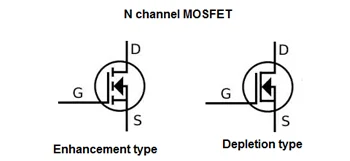
Before, we go over the construction of P-Channel MOSFETs, we must go over the 2 types that exist. There are 2 types of P-Channel MOSFETs, enhancement-type MOSFETs and depletion-type MOSFETs.
A depletion-type MOSFET is normally on (maximum current flows from source to drain) when no difference in voltage exists between the gate and source terminals. However, if a voltage is applied to its gate lead, the drain-source channel becomes more resistive, until the gate voltage is so high, the transistor completely shuts off. An enhancement-type MOSFET is the opposite. It is normally off when the gate-source voltage is 0V (VGS=0). However, if a voltage is applied to its gate lead, the drain-source channel becomes less resistive.
What is JFET?
JFET is the simplest type of field-effect transistor in which the current can either pass from source to drain or drain to source. Unlike bipolar junction transistors (BJTs), JFET uses the voltage applied to the gate terminal to control the current flowing through the channel between the drain and source terminals which results in output current being proportional to the input voltage. The gate terminal is reverse-biased. It’s a three-terminal unipolar semiconductor device used in electronic switches, resistors, and amplifiers. It anticipates a high degree of isolation between input and output which makes it more stable than a bipolar junction transistor. Unlike BJTs, the amount of current allowed is determined by a voltage signal in a JFET.
It’s generally classified into two basic configurations:
N-Channel JFET – The current flowing through the channel between the drain and source is negative in the form of electrons. It has lower resistance than P-Channel types.
P-Channel JFET – The current flowing though the channel is positive in the form of Holes. It has higher resistance than its N-Channel counterparts.
What is MOSFET?
MOSFET is a four-terminal semiconductor field effect transistor fabricated by the controlled oxidation of silicon and where the applied voltage determines the electrical conductivity of a device. MOSFET stands for Metal Oxide Semiconductor Field Effect Transistor. The gate which is located between the source and drain channels is electrically insulated from the channel by a thin layer of metal oxide. The idea is to control the voltage and current flow between the source and drain channels. MOSFETs play a vital role in integrated circuits because of their high input impedance. They are mostly used in power amplifiers and switches, plus they play a critical role in embedded system design as functional elements.
They are generally classified into two configurations:
Depletion Mode MOSFET – The devices are normally “ON” when the gate-to-source voltage is zero. The application voltage is lower than the drain-to-source voltage
Enhancement Mode MOSFET – The devices are normally “OFF” when the gate-to-source voltage is zero.
What is Half Wave Rectifier?
In a half-wave rectifier, one half of each a.c input cycle is rectified. When the p-n junction diode is forward biased, it gives little resistance and when it is reversing biased it provides high resistance. During one-half cycles, the diode is forward biased when the input voltage is applied and in the opposite half cycle, it is reverse biased. During alternate half-cycles, the optimum result can be obtained.
Working of Half Wave Rectifier
The half-wave rectifier has both positive and negative cycles. During the positive half of the input, the current will flow from positive to negative which will generate only a positive half cycle of the a.c supply. When a.c supply is applied to the transformer, the voltage will be decreasing at the secondary winding of the diode. All the variations in the a.c supply will reduce, and we will get the pulsating d.c voltage to the load resistor.
What is Full Wave Rectifier?
Full-wave rectifier circuits are used for producing an output voltage or output current which is purely DC. The main advantage of a full-wave rectifier over half-wave rectifier is that such as the average output voltage is higher in full-wave rectifier, there is less ripple produced in full-wave rectifier when compared to the half-wave rectifier.
Working of Full Wave Rectifier
The full-wave rectifier utilizes both halves of each a.c input. When the p-n junction is forward biased, the diode offers low resistance and when it is reversing biased it gives high resistance. The circuit is designed in such a manner that in the first half cycle if the diode is forward biased then in the second half cycle it is reverse biased and so on.
LC Filters
LC filters refer to circuits consisting of a combination of inductors (L) and capacitors (C) to cut or pass specific frequency bands of an electric signal.
Capacitors block DC currents but pass AC more easily at higher frequencies. Conversely, inductors pass DC currents as they are, but pass AC less easily at higher frequencies.
In other words, capacitors and inductors are passive components with completely opposite properties. By combining these components with opposite properties, noise can be cut and specific signals can be identified.
Types of LC Filters
LC filters are broadly classified into three types.
Low-pass Filters(LPF)
Low-pass filters are filter circuits that pass DC and low-frequency signals and cut high-frequency signals.
They are the most widely used filter circuits and are mainly used to cut high-frequency noise.
In audio, they are also used to cut treble/mid-range sound components of bass speakers.
High-pass Filters (HPF)
High-pass filters are filter circuits that cut DC and low-frequency signals and pass high-frequency signals.
They are used to cut low-frequency noise in the audible range, cut mid-range/bass sound components of treble speakers, etc.
Band-pass Filters (BPF)
Band-pass filters are filter circuits that pass only signals at a specific frequency and cut signals at other frequencies.
They are used for radio tuning (frequency adjustment) or for cutting the bass/treble sound components of mid-range speakers, etc.
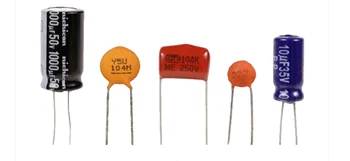
Capacitor
A capacitor is a device that stores electrical energy in an electric field. It is a passive electronic component with two terminals.
The effect of a capacitor is known as capacitance. While some capacitance exists between any two electrical conductors in proximity in a circuit, a capacitor is a component designed to add capacitance to a circuit. The capacitor was originally known as a condenser or condensator. This name and its cognates are still widely used in many languages, but rarely in English, one notable exception being condenser microphones, also called capacitor microphones.
The physical form and construction of practical capacitors vary widely and many types of capacitor are in common use. Most capacitors contain at least two electrical conductors often in the form of metallic plates or surfaces separated by a dielectric medium. A conductor may be a foil, thin film, sintered bead of metal, or an electrolyte. The nonconducting dielectric acts to increase the capacitor's charge capacity. Materials commonly used as dielectrics include glass, ceramic, plastic film, paper, mica, air, and oxide layers. Capacitors are widely used as parts of electrical circuits in many common electrical devices. Unlike a resistor, an ideal capacitor does not dissipate energy, although real-life capacitors do dissipate a small amount (see Non-ideal behavior). When an electric potential difference (a voltage) is applied across the terminals of a capacitor, for example when a capacitor is connected across a battery, an electric field develops across the dielectric, causing a net positive charge to collect on one plate and net negative charge to collect on the other plate. No current actually flows through the dielectric. However, there is a flow of charge through the source circuit. If the condition is maintained sufficiently long, the current through the source circuit ceases. If a time-varying voltage is applied across the leads of the capacitor, the source experiences an ongoing current due to the charging and discharging cycles of the capacitor.
The earliest forms of capacitors were created in the 1740s, when European experimenters discovered that electric charge could be stored in water-filled glass jars that came to be known as Leyden jars. Today, capacitors are widely used in electronic circuits for blocking direct current while allowing alternating current to pass. In analog filter networks, they smooth the output of power supplies. In resonant circuits they tune radios to particular frequencies. In electric power transmission systems, they stabilize voltage and power flow. The property of energy storage in capacitors was exploited as dynamic memory in early digital computers, and still is in modern DRAM.
Inductor
An inductor, also called a coil, choke, or reactor, is a passive two-terminal electrical component that stores energy in a magnetic field when electric current flows through it. An inductor typically consists of an insulated wire wound into a coil.
When the current flowing through the coil changes, the time-varying magnetic field induces an electromotive force (e.m.f.) (voltage) in the conductor, described by Faraday's law of induction. According to Lenz's law, the induced voltage has a polarity (direction) which opposes the change in current that created it. As a result, inductors oppose any changes in current through them.
An inductor is characterized by its inductance, which is the ratio of the voltage to the rate of change of current. In the International System of Units (SI), the unit of inductance is the henry (H) named for 19th century American scientist Joseph Henry. In the measurement of magnetic circuits, it is equivalent to weber/ampere. Inductors have values that typically range from 1 µH (10−6 H) to 20 H. Many inductors have a magnetic core made of iron or ferrite inside the coil, which serves to increase the magnetic field and thus the inductance. Along with capacitors and resistors, inductors are one of the three passive linear circuit elements that make up electronic circuits. Inductors are widely used in alternating current (AC) electronic equipment, particularly in radio equipment. They are used to block AC while allowing DC to pass; inductors designed for this purpose are called chokes. They are also used in electronic filters to separate signals of different frequencies, and in combination with capacitors to make tuned circuits, used to tune radio and TV receivers.

![Study Material | Electronic Circuits | Demonstrator in Electronics and Instrumentation [ Cat No. 295/2021, 296/2021]](https://blogger.googleusercontent.com/img/a/AVvXsEiqA9gj6xPSqB_Y2g2Z6_fEoXBQclr36QKyiqz87UNAlKDrLzcVVeW0B5_9bSmkdyp-cXV8qo-lPmVFRC7KLmc-asiuF3n7ajPL0wHmPgKkNBOBKHpDm3h43N_Tx7zNhWc0m62N3aFjArFaHasqubt4cukF5njFvTmMfLYc2PzPpfLPlw8eV7VYybr0Fw=rw)


0 Comments